High Resolution Raman shift and bandwidth images of stressed silicon

16. High Resolution Raman Shift and Bandwidth Images of Stressed Silicon
Michael Bowden and Derek J Gardiner
Department of Chemical and Life Sciences, University of Northumbria at Newcastle, Ellison Place, Newcastle upon Tyne, UK, NE1 8ST.
E-Mail Derek.Gardiner [at] UNN.AC.UK
Abstract
This feature article sets out to describe some important materials science applications of Raman imaging. In addition we illustrate the value of using images to reveal spatially significant, spectral changes which might otherwise be overlooked. Stress fields in micro-indented silicon, edge stresses associated with thin film pads and temperature variations in polysilicon heater devices are discussed as examples.
Introduction
Raman microscope imaging was first demonstrated by Delhaye and Dhamelincourt [1] in 1974. A double monochromator with non-astigmatic gratings was used as a relatively wide bandpass filter to select the required Raman shift frequencies and the image was captured on a vidicon detector. The technique, though an important milestone, was of limited value and only worked well with strong Raman scatterers and where narrow frequency band image selection was not required. The routine generation of micro-Raman images became achievable with the development of the ccd detector. An instrument employing tunable bandpass filters to select Raman scattered light from a globally illuminated sample and to image it onto a cooled slow scan ccd detector was first described by Batchelder [2] in 1992. Various attempts have also been made to generate Raman images from point by point collection of an array of spectral data [3].
The Microline Focus Spectrometer (MiFS) which we have developed has been described in detail elsewhere [4, 5]. The instrument uses cylindrical optics to produce a line focus of the incident laser beam on the surface of the sample. Light scattered from this line is then imaged through a subtractive filter stage to remove the incident laser frequency and a spectrograph stage to form a spectrally dispersed image of the Raman scatter on a cooled ccd detector. The non-astigmatic imaging optics employed ensure that the spatial integrity of the origin of the scattered light is retained, thus generating Raman data from the length of the focused laser line at a single exposure. Raman images are obtained by collecting data from a series of adjacent lines on the sample surface. The process is summarised in Figure 1. Raman spectra are dispersed on the ccd chip (lambda), with y as the spatial direction. At each line position on the sample (x) the required spectral parameters are extracted and manipulated to remove background, determine integrated intensity (Iy), position (ry) and bandwidth at half height (by). These data are then written as a greyscale image to a monitor screen before moving on to the next line position. In this way the Raman image is generated in near real time whilst at the same time the full dynamic range of the image data is retained for three dimensional plotting or for further analysis. This approach is an objective compromise between the time consuming and high positional stability demands of point by point sampling of the surface and the spectroscopically limited global illumination method. In addition the method does not rely upon moving optical components and thus is inherently stable. Systematic error in the spectral data is also eliminated and the inclusion of a convenient laser plasma line allows high precision Raman shift data to be realised.
Stress variations and structural defects in bulk silicon are of concern to developments in microelectronics and more recently in microengineering structures. In the former, stress is generated as a consequence of epitaxial growth and the varying architecture of component device layers, whilst in the latter, stress variations may arise from high doping levels and from etch removal of bulk silicon to produce the required microstructure. The response of the silicon Raman spectrum to stress and temperature has been reviewed [6], along with the use of Raman microscopy to determine the spatial variation of these parameters [7]. Much of the Raman microscopy work to date has used single point probing to explore the spatial variations in silicon structures with the result that only limited Raman data can be obtained and evaluated within a reasonable time. The development of Raman imaging instruments makes it possible to collect large Raman data sets over a surface area and to process these into stress and structure characteristic images, at high spatial and spectral resolution within an acceptable time-scale. Here we show how the results of applied stress and temperature can be visualised using Raman shift and bandwidth images.
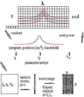
Figure 1. Schematic of the MiFS mapping/imaging process
Theoretical aspects
Pure single crystal silicon is cubic, belongs to the crystal symmetry class Oh and gives rise to a single triply degenerate Raman active T2g phonon mode at around 520 cm-1. Amorphous silicon gives rise to broad features at 140 and 475 cm-1. Polysilicon or microcrystalline silicon formed by CVD methods, gives rise to a broader band around 518 cm-1, often with additional structure on the low frequency side dependent upon the deposition conditions. The application of an in-plane, biaxial compressive stress results in a positive shift of the phonon frequency, while tensile stress produces a negative shift. Extreme stresses such as those developed under the high impact loads experienced adjacent to an indenter tool, or as a result of surface scratching [8], can result in splitting and asymmetry of the phonon band. This response can be variously interpreted as indications of regions retaining a high degree of non-isotropic strain, or the development of metastable silicon phases.
Increase in temperature decreases the phonon relaxation time and alters the phonon state population with the result that the phonon band shifts to lower frequencies and broadens with increasing temperature.
Experimental
The Raman spectra were excited using either the 488nm or the 514.5nm line from an Ar+ laser generating around 5-10 mW at the sample. The incident beam was polarised parallel to the sample x direction and in the work presented here no analyser was used and all the scattered light was detected. Objectives of 40x and 100x magnification were used producing line lengths of 120 µm or 50 µm respectively on the sample. When the 488nm line was employed, a convenient laser plasma line at 529.66 cm-1 shift was used as a reference.
Compression and fracture mapping in micro-indented silicon
The images of Figure 2 were obtained from the (001) surface of crystalline silicon indented with a Vickers micro-indenter using a square pyramidal diamond tip with a load of 0.1N applied for 15 seconds. The diagonals of the indenter tip were aligned with the <100> direction. The white light image of the damage site showed only a small ~3 µm wide square indentation. The Raman shift image (Figure 2a) in which white represents a positive and black a negative shift, reveals extensive regions due to compressive modification adjacent to the edges of the indent and extending symmetrically for 2-3 µm. Between these regions and radiating from the corners of the indent are darker areas arising from silicon under tension. No evidence of cracking is apparent. Figure 2b confirms that the phonon bandwidth is most affected close to the indent edges where it is assumed some structural modification has occurred.
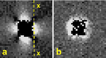
Figure 2. Raman images of a 12µm square indent damage site (a) Raman shift (b) halfbandwidth
The three dimensional plot of Figure 3 is an alternative presentation of the same data and shows the compressive and tensile regions. The scale of the phonon frequency changes which were observed are made clear in Figure 4 which is a plot of the cross section (xx) indicated in Figure 2a. Here the relative scale of the tensile and compressive frequency responses can be seen, which cover a range of around 4 cm-1.
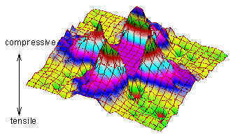
Figure 3. Three dimensional plot of the data of Figure 2a
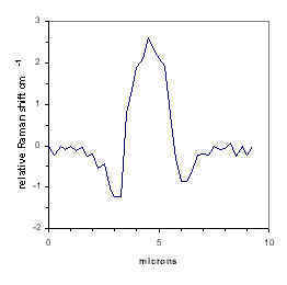
Figure 4. Section xx from Figure 2a
The Raman shift images (a,b,c) and the corresonding halfbandwidth images (d,e,f) shown in Figure 5 arise from higher load indents and reveal varying amounts of cracking. Raman shift images show compressive regions as before, but at the crack tips, small, dark, tensile regions can be seen, consistent with crack propagation. The halfbandwidth images appear to indicate incipient lateral crack or flake formation. Figure 5d in which the indent diagonals are aligned with the <110> direction (the most favourable cleave direction) identifies a ring of structural damage at the crack radius. A similar result is seen in Figure 5f. The image of Figure 5e results from an indent where the diagonals were aligned with the <100> direction. Here the cracking is more complex, tending to follow the <110> direction and a well developed lateral crack, which is a precursor to flaking can be observed in the lower right hand quadrant. The indent of Figure 6 has resulted in flake formation indicated by the region of low strain on the right hand side (Figure 6a) with structural damage indicated by the increased bandwidth (Figure 6b) around the perimeter of the flake.
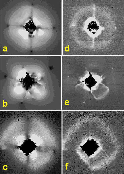
Figure 5. Raman images of 50 µm square regions around indent damage sites. (a,b,c) Raman shift, (d,e,f) halfbandwidth.
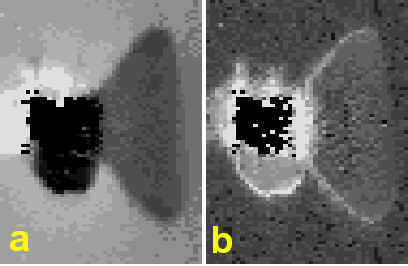
Figure 6. Raman images of a 12 x 20 µm region around an indent damamge site showing flake formation.
Silicon Nitride Pad Edge Effects in Silicon
It is well established that thin films, deposited on silicon, will exhibit varying degrees of stress. When the thin films are deposited as pads, then the silicon substrate will experience stresses at the pad edge [9]. We have investigated this effect by studying a checkerboard of 10mm square silicon nitride pads deposited on silicon (100) under a range of conditions. Initial experiments involved using single exposures, with the line focus at a small angle to the pad edge in order to increase the pixel resolution in the spatial direction. A typical result is shown in Figure 7. In the clear silicon region a constant phonon frequency of 520.7 cm-1 is observed until at around 10 µm from the edge the frequency begins to increase, reaching a maximum of 521.0 cm-1. Under the pad the frequency drops rapidly over the next 1µm to 520.5 cm-1 and then returns to 520.7 cm-1 over the next 10 µm.
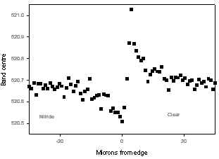
Figure 7. Plot of phonon frequency as a function of distance across a silicon nitride pad edge.
The three dimensional plot displayed in Figure 8 was obtained from the same sample by mapping over the corners of two proximate pads as indicated. The Raman shift data has been adjusted to show tensile stresses as positive in the vertical direction and compressive stresses as negative, in line with convention. The stress trough around the edges of the pad is clearly discernible. Other checkerboard samples prepared with pad stresses from tensile to compressive were studied and revealed complementary results. A sample produced with no pad stress showed no edge effects.
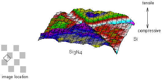
Figure 8. Silicon strain image of a 15 x 18 µm region around two silicon nitride pad corners showing edge effects
Temperature mapping of polysilicon heaters
As described in the introduction, the polysilicon phonon band changes dramatically with temperature. The effect over 600° C is illustrated in Figure 9.
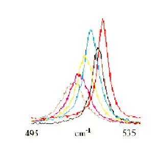
Figure 9. Polysilicon phonon spectra over a range of temperatures from 25°C (red) to 600°C (grey)
As the temperature rises from room temperature (red trace) to 600° C (grey trace) the frequency decreases as the bandwidth increases. The intensity variations arise from the refocusing required at each temperature and changes in the density of states distribution as the temperature increases. The frequency change over this range is linear as shown in the plot of Figure 10 and can be used to monitor temperature.

Figure 10. Plot of Raman shift data from Figure 9 with linear regression line.
As an example of this application, which is discussed in more detail elsewhere [10], the MiFS mapping procedure was used to produce a Raman shift image of a working polysilicon micro-heater composed of a free standing polysilicon meander anchored at each end to a contact pad. The data was then transformed using the results of Figure 10 to produce the temperature image shown in Figure 11. The temperature can be seen to increase from ambient to around 350° C at the centre of the meander.
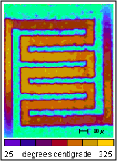
Figure 11. Temperature image of a polysilicon micro-heater
Conclusions
The Raman imaging applications described here demonstrate the value of using image data to detect subtle, spatially significant, spectral changes. It is the patterns revealed in a complete image which lend significance to small spectral variations The bandwidth halos in Figures 5d and 5f, the flake in Figure 6 and the stress trough in Figure 8, are strikingly revealed but might only be discernible from individual point measurements following extensive repeat measurements and data analysis.
Acknowledgements
DERA (Malvern) for supply of the micro-heaters and preparation of the silicon nitride checkerboard samples
References
- M. Delhaye and P. Dhamelincourt, IVth Internat. Conf. Raman Spectrosc.,Brunswick,ME, USA, (1974). D. N. Batchelder, Measurement Sci. and Technol., 3, 561, (1992).
- M. Bowden, G.R.Dickson, D.J.Gardiner and D.J.Wood, Appl. Spectrosc., 44, 1679, (1990).
- M. Bowden, D. J. Gardiner and J. M. Southall, J. Appl. Phys., 71, 521, (1992).
- M. Bowden and D. J. Gardiner, Appl. Spectrosc., 51, 1405, (1997).
- F. H. Pollak, Analytical Raman Spectroscopy, Ed. J. G. Grasselli and B. Bulkin, Chemical Analysis Series, 114, J Wiley (1991), ISNB 0-471 51955-3
- I. DeWolf, Semicond. Sci. Technol., 11, 139-154,(1996).
- S. Webster, D. N. Batchelder and D. A. Smith, Appl. Phys. Lett., 72, 1478, (1998).
- J. Vanhhellemont and S. Amelinckx, J. Appl. Phys., 61, 2170, (1987).
- M. Bowden, D. J. Gardiner, A. A. Parr, R. T. Carline, R. J. Bozeat, R. J. T. Bunyan and M. Ward, Microsc. Inst. Phys. Conf. Ser., 157, 439, (1997).
Received 27th April 1998, received in revised format 22nd May 1998, accepted 18th May 1998.