Integrated Raman Analyzer Using Volume Holographic Optical Elements
M. J. Pelletier
Kaiser Optical Systems, Inc.,
371 Parkland Plaza, Ann Arbor, MI 48103 USA
pelletier [at] kosi.com, http://www.kosi.com
Introduction
In the recent past Raman spectrometers were generally thought of as laboratory instruments only. They were not designed to withstand the demands of industrial process analysis and control. Industrial process analysis and control instruments often need to operate reliably and continuously with little supervision or maintenance. Vibration, temperature variation, dirtiness, and limited access to the sample are often an unavoidable part of this environment. Common laboratory utilities, such as cooling water, high power electrical service, liquid nitrogen, and people familiar with analytical instrumentation, are often not available. Raman instruments of the past were simply not acceptable as process analyzers.
Recent developments in optical, laser, and detector technology have made possible a new generation of Raman instruments. These Raman instruments meet the demands of industrial process analysis and control, and still provide the performance of state-of-the-art laboratory instruments. This report will describe one such instrument, the Kaiser Optical Systems HoloProbe.
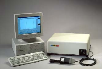
Figure 1: The HoloProbe, an integrated Raman Instrument.
A photograph of the integrated Raman system is shown in Figure 1. It consists of a computer, a base unit having a 23 inch by 18 inch footprint, and a probehead. The computer is connected to the base unit by a single high speed serial cable. The probehead is connected to the base unit by a single cable that contains two optical fibers. This fiber optic cable may be any length from 1.9 meters to greater than 100 meters. Raman spectra are collected by pointing the probehead at the sample, and clicking the acquire button.
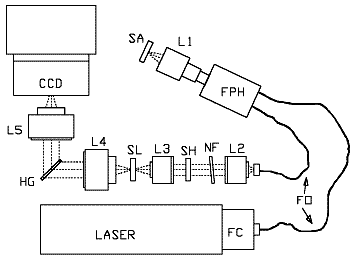
Figure 2: Schematic drawing of the HoloProbe base unit with fiber optic probe head attached.
FC, fiber optic coupler; FO, fiber optic cable (1.9 meter length standard); FPH, fiber optic probe head; L1, focus and collection lens; SA, sample; L2, pre-filter collimating lens; NF, holographic notch filter; SH, shutter; L3, pre-filter focusing lens; SL, spectrograph entrance slit; L4, spectrograph collimating lens; HG, HoloPlex grating; L5, spectrograph focusing lens.
A schematic diagram of the instrument is shown in Figure 2. Light from the laser is coupled into a probehead through an optical fiber. The probehead illuminates the sample and collects Raman scattered light from the sample. The Raman scattered light is sent back to the base unit through a second optical fiber. In the base unit, residual laser light is removed and the Raman light is spectrally dispersed onto a CCD detector. The signal generated from the image on the CCD detector is sent to the computer for conversion into a spectrum. HoloGRAMS software is used for instrument configuration and control. HoloGRAMS also works with other software packages such as GRAMS, Excel, or Spectacle through the Windows DDE interface.
The HoloProbe design represents a significant departure from traditional Raman instrument design. Traditional laboratory Raman instruments based on triple spectrographs are extremely flexible instruments. They are designed to operate with a wide range of excitation wavelengths, spectral resolutions, and instrumental configurations. The price for this flexibility is compromised performance and increased complexity. The HoloProbe design gives up much of this flexibility in exchange for improved performance, simpler, more stable alignment, and easier coupling to the sample.
The critical components and assemblies that make up the HoloProbe are described in greater detail in the following sections of this paper.
CCD detector
The CCD detector [1] is actually a two dimensional array of nearly ideal detectors called pixels. Each pixel is a silicon detector. Photons absorbed by the pixel silicon release electrons that accumulate in that pixel. When the CCD detector is “read out”, the total accumulated charge in each pixel is determined. Values proportional to the charge in each pixel are stored in the computer for further analysis. More detailed description of CCD detector design, operation, and performance have been published [2-6].
In nearly all practical cases the noise from the CCD detector is much lower than shot noise, the statistical noise due to the quantum nature of light itself. The signal-to-noise ratio of Raman spectra collected with a CCD detector is therefore proportional to the square root of the number of detected photons. Raman photons are usually in short supply, so increasing the number of detected Raman photons will usually increase the Raman instrument sensitivity and quantitative accuracy.
The standard CCD detector used in the HoloProbe is a rectangular array of 1024 by 256 pixels. Since each pixel is an independent detector, more than 250,000 independent measurements can be made simultaneously. The HoloProbe uses the massively parallel detection capability of the CCD detector to measure all of the wavelengths in the Raman spectrum simultaneously and continuously during the data acquisition time. In fact, a four channel adapter allows the HoloProbe to simultaneously measure the complete Raman spectra from 4 independent points. Simultaneous measurement of all wavelengths eliminates sampling artifacts that occur in single-channel or multiplex detection systems when the spectrum changes during a single scan. Simultaneous measurement therefore gives the HoloProbe immunity to artifacts generated by laser noise, bubbles, turbulence, or moving samples.
An important limitation of CCD detectors is the small size of their pixels. The standard CCD detector used in the HoloProbe has square pixels 27 microns on a side. The HoloProbe combines the signal of several pixels into a single “super pixel” in order to make the effective detector size larger, but even so, super pixels are still very small. As a result, not only does the Raman instrument need to deliver as many Raman photons as possible to the CCD detector, the instrument must also concentrate those photons into a very small area. These two goals define the major design objectives for the HoloProbe spectrograph.
Spectrograph
The spectrograph section in the base unit disperses light from the filter stage into a spectrum and images the spectrum onto a CCD detector. The spectrograph is an axial transmissive design [2], rather than the more traditional Czerny-Turner design. These two designs are compared in Figure 3. The axial transmissive spectrograph design uses lenses instead of mirrors in order to get good imaging quality with an aperture ratio (focal length divided by focusing optic diameter) of f/1.8. The light gathering ability at the detector decreases with the square of aperture ratio, so lens-based spectrographs with small focal ratios give higher optical throughput to CCD detectors [3].

Figure 3: Axial transmissive spectrograph configuration, left, and Czerny-Turner spectrograph configuration, right.
Traditional Raman spectrographs operate in the f/5 to f/8 range or higher in order to achieve acceptable imaging quality and linear dispersion with simple spherical or toroidal mirrors. Image blurring at the detector increases rapidly as the focal ratio is reduced. Even at f/4 the imaging quality of a Czerny-Turner spectrograph is much worse than that of an axial transmissive design. This blurring degrades the spectral resolution of the Raman instrument, limits the number of independent measurements channels, and decreases Raman peak heights.
The axial transmissive spectrograph also uses a unique volume holographic transmission grating [9] discussed later in this paper, that stacks two spectral regions on top of each other at the detector, effectively doubling the spectral coverage that can be obtained with a given CCD detector. Since the entire spectrum is imaged on the CCD detector simultaneously, there is no need to ever move the grating. The elimination of grating movement and adjustment hardware simplifies the spectrograph and removes a potential source of misalignment and failure. Unlike traditionally used reflection gratings, the transmission grating produces only a small spectral shift at the detector when the grating angle is changed. This property makes the axial transmissive spectrograph wavelength calibration more stable than a typical spectrograph using reflection gratings.
The diffraction grating used by the HoloProbe needs to have a very large angular dispersion due to the short focal length (85 mm) of the spectrograph. Angular dispersion refers to the different directions light of different wavelengths takes as it leaves the diffraction grating. High angular dispersion often causes some diffracted light to get lost because it spreads out too quickly to be fully captured by the spectrograph focusing lens (or mirror). This kind of light loss is called vignetting. The axial transmissive spectrograph design minimizes vignetting by placing the focusing lens very close to the grating.
Optical Fibers and the Fiber optic Probehead
Raman light is delivered to the base unit by an optical fiber having a core diameter of 100 micrometers and a numerical aperture of 0.29. It is this relatively large diameter and large numerical aperture that makes the low focal ratio of the spectrograph so important. A spectrograph having a larger focal ratio cannot efficiently deliver the light from the optical fiber to a target as small as the CCD pixels. The amount of light that can be coupled from the sample into the optical fiber increases with core diameter and numerical aperture, though. Probehead alignment tolerances also increase with fiber core diameter, so it is usually advantageous to use the largest collection fiber that the spectrograph can efficiently handle.
 Figure 4: Schematic diagram of the HoloProbe fiber optic probehead.
The HoloProbe fiber optic probehead [10,11] is described in detail, along with other fiber optic probe designs, by Lewis et al. [12,13], so it will be described only briefly here. A schematic diagram of the probehead is shown in Figure 4. The probehead uses the same detachable optic to focus laser light on the sample, and to collect Raman emission from the sample. Permanent alignment inside the probehead ensures that the excitation optical path and the collection optical path are always properly aligned, regardless of the collection optic used. Numerous collection optics are available to provide the user with a wide range of working distances and interfaces to process equipment. For example, one class of collection optics consists of a lens and window in a hollow tube. This optic can be immersed in transparent or opaque liquids. It is automatically optimally focused on the sample. No optical alignment is required from the user.
Laser light is delivered to the probehead by a single optical fiber. This laser light is contaminated by fluorescence and Raman emission from the optical fiber itself. The probehead therefore contains a miniature volume holographic monochromator to filter this contamination from the laser light. Light scattered by the sample is coupled into the second optical fiber, but only after it is filtered by a volume holographic notch filter to reject laser light scattered by the sample. If this laser light were coupled into the second optical fiber, it would produce fluorescence and Raman emission from the second optical fiber that would interfere with the Raman signal from the sample.
Holographic Optical Elements
The HoloProbe uses several high performance volume holographic optical elements (HOEs). These relatively new devices consist of a volume hologram in a thin film of dichromated gelatin that is sealed between two plates of glass [14]. The hologram is an optical interference pattern recorded as refractive index variations in the gelatin. Unlike artistic holograms, which produce 3-dimensional images, the hologram(s) in HOEs simulate optical devices or combinations of optical devices. This technology has been used in military fighter aircraft for many years, but only recently became available to the spectroscopic community.
Volume holographic notch filters are used in both the base unit and in the probehead to reject laser light while efficiently transmitting Raman light. They offer a simple, small, less expensive, higher throughput, and more mechanically robust alternative to the traditional subtractive double spectrograph. Volume holographic notch filters do not distort Raman spectra the way that dielectric filters or subtractive double spectrographs do because the volume holographic notch filter transmission curves are very smooth and flat throughout nearly all of the Raman spectral region. Volume holographic notch filters transmit Raman light as close as 50 cm-1 from the laser line while reducing the intensity at the laser wavelength by more than a factor of one million.
A volume holographic beam splitter is used in the fiber optic probehead to combine the excitation and collection paths. This beam splitter is really just another volume holographic notch filter.
Volume holographic diffraction gratings are used in the miniature monochromator inside the fiber optic probehead, and in the 785 nm laser filter. In addition to their high diffraction efficiency, these gratings have much lower optical absorption than metal reflection gratings, and therefore a much higher laser damage threshold. These gratings are exposed to the full laser power, so high damage threshold can be as important as high throughput.
Finally, the most complex volume holographic optical element in the HoloProbe is the diffraction grating in the spectrograph section described earlier.
Lasers
The HoloProbe is configured with one of four different types of laser: a 532 nm frequency-doubled Nd:YAG laser, a 785 nm external cavity stabilized diode laser, a 1064 nm Nd:YAG laser, or a 633 nm HeNe laser. Each of these lasers has no need for alignment or maintenance for the entire lifetime of the laser, which tends to be one year or longer of continuous operation. A volume holographic laser bandpass filter is used with the diode laser to reject the intense superradiant emission. Without this filter, the superradiant emission can add an overwhelming continuum background to the low wavenumber region of the Raman spectrum. Lasers external to the HoloProbe base unit can also be used by coupling them directly into the laser delivery fiber that normally attaches to the HoloProbe base unit.
Base unit filter stage
Light from the collection optical fiber entering the base unit first passes through the filter stage. The filter stage uses a volume holographic notch filter to remove residual laser light. It also contains a shutter to control the data acquisition time, and a lens to focus the Raman light onto the entrance slit of the spectrograph.
The fiber optic connector that couples the optical fiber to the base unit is mounted on a plate that is kinematically mounted to the filter stage. This plate snaps in and out of the filter stage. It can be replaced with a 4 channel adapter that accepts four fiber optic cables, and directs their outputs through the filter stage to the proper locations on the spectrograph entrance slit.
Raman Applications
Raman spectroscopy was traditionally confined to the laboratory environment. The instrument described in this paper, however, is being used in many applications outside the laboratory environment. In most cases, the primary reason for choosing Raman spectroscopy for these applications over any other analytical technique was ease of sampling. Raman spectroscopy provides detailed analytical results without collecting or diverting a sample from the process.
Raman spectroscopy provides non-invasive, non-contact, non-destructive analysis through common window materials such as glass, sapphire, or quartz. It can often be made insensitive to films that build up on windows by simply focusing at a point further from the window. Fiber optic probes allow the Raman instrument to be hundreds of meters away from the actual point of measurement.
A detailed discussion of specific Raman applications is beyond the scope of this paper. A few brief descriptions of representative (and non-proprietary) applications, however, should illustrate the types of analytical problems that are well suited to Raman spectroscopy.
Raman spectroscopy is being used to continuously monitor the contents of the reaction vessel used to manufacture PCl3 [15]. The Raman probe is held inside the reaction vessel. The previous analytical method required pumping the contents of the reaction vessel through an external flow cell and back into the reactor. While this sounds like an easy thing to do, the hazardous nature of the reactor contents made the external flow cell approach very expensive and undesirable. The in-situ Raman measurement provides the required analytical data in a safe, cost-effective, and low-maintenance manner.
Raman spectroscopy is being used to replace gas chromatography in a distillation monitoring application [16]. In this case, the lower maintenance costs and supplies costs made the estimated total cost-of-ownership lower for Raman spectroscopy than for gas chromatography. Faster analytical results were an added benefit that provided unexpected insight into the true operation of the distillation column.
Raman spectroscopy was used to non-destructively determine the integrity of micromechanical silicon accelerometer chip seals [17]. The analytical challenge was to quantitatively analyze the gas in a 70-micron-deep cavity between a silicon cap and a Pyrex window.
One final example is the use of Raman spectroscopy to monitor the composition of semiconductor cleaning baths [18]. In this case the analysis had to be non-contact in order to avoid any possibility of contaminating the ultra-pure cleaning reagents. The cleaning solution generated a continuous stream of bubbles, so the measured Raman signal intensity varied randomly over a wide range. The quantitation accuracy was better than 0.1%, however, because all of the Raman wavelengths were simultaneously and continuously measured.
References
1. J. V. Sweedler, Charge Transfer Device Detectors and Their Applications to Chemical Analysis, Crit. Rev. Anal. Chem. 24, 59 (1993).
2. R. B. Bilhorn, P. M. Epperson, J. V. Sweedler, and M. B. Denton, Spectrochemical Measurements with Multichannel Integrating Detectors, Appl.Spectrosc.41., 1125 (1987).
3. J. V. Sweedler, R. B. Bilhorn, P. M. Epperson, G. R. Sims and M. B. Denton, High Performance Charge Transfer Device Detectors, Anal.Chem. 60, 283A (1988).
4. P. M. Epperson, J. V. Sweedler, R. B. Bilhorn, G. R. Sims, and M. B. Denton, Applications of Charge Transfer Devices in Spectroscopy, Anal.Chem. 60, 327A (1988).
5. J. E. Pemberton, R. L. Sobocinski, M. A. Bryant, and D. A. Carter, Raman Spectroscopy using Charge-Coupled Device Detection, Spectroscopy 5, 26 (1990).
6. J. V. Sweedler, K. L. Ratzlaff, and M. B. Denton, Charge-Transfer Devices in Spectroscopy, VCH Publishers, New York, NY, 1994.
7. D. E. Battey, J. B. Slater, R. Wludyka, H. Owen, D. M. Pallister, and M. D. Morris, Axial Transmissive f/1.8 Imaging Raman Spectrograph with Volume-Phase Holographic Filter and Grating, Appl. Spectrosc. 47, 1913 (1993).
8. M. J. Pelletier, Raman Spectroscopy Using an Echelle Spectrograph with CCD Detection, Appl. Spectrosc. 44, 1699 (1990).
9. U. S. Patent 5,559,597, Spectrograph with Multiplexing of Different Wavelength Regions onto a Single Opto-Electric Detector Array, Sept 24, 1997.
10. U. S. Patent 5,377,004, Remote Optical Measurement Probe, December 27, 1994.
11. H. Owen, D. E. Battey, M. J. Pelletier, and J. B. Slater, New Spectroscopic Instrument Based on Volume Holographic Optical Elements, SPIE Vol 2406, 260 (1995).
12. I. R. Lewis and P. R. Griffiths, Raman Spectroscopy with Fiber-Optic Sampling, Appl.Spectrosc. 50, 12A (1997).
13. I. R. Lewis and P. R. Griffiths, to be published in this journal.
14. J. M. Tedesco, H. Owen, D. M. Pallister, and M. D. Morris, Principles and Spectroscopic Applications of Volume Holographic Optics, Anal. Chem. 65, 441A (1993).
15. G. Gervasio and M. J. Pelletier, On-Line Raman Analysis of PC13 Reactor Material, Tenth International Forum Process Analytical Chemistry, Haines City, Florida, January 21-24, 1997.
16. E.D. Lipp and R.L. Grosse, Analysis of Chlorosilane Process Streams by Raman Spectroscopy, XVth International Conference on Raman Spectroscopy, Pittsburgh, PA, August 11-16, 1996.
17. W.H. Weber, M. Zanini-Fisher and M.J. Pelletier, Using Raman Microscopy to Detect Leaks in Micromechanical Silicon Structures, Appl. Spectrosc. 51, 123 (1997).
18. M.J. Pelletier, K.L. Davis and R.A. Carpio, Applications of Raman Spectroscopy for SC-1 Processing Bath Concentration Contol, Proc. Electrochem. Soc. 95-2, 282 (1995).
REF: Int. J. Vib. Spect., [www.irdg.org/ijvs] 1, 3, 4 (1997)