Raman Microscopy of Technical Ceramics: Silicon Infiltrated Silicon Carbide

5. Raman Microscopy of Technical Ceramics: Silicon Infiltrated Silicon Carbide
Jan-Christoph Panitz
Paul Scherrer Institut
OFLC 107/A
CH-5232 Villigen PSI
Tel: +41 56 310 41 94
Fax.: +41 56 310 21 99
E-mail: Jan-Christoph.Panitz [at] psi.ch
Keywords
Raman microscopy, composite ceramic materials, silicon, silicon carbide
Introduction
Technical ceramics made of silicon carbide play a key role as materials for high temperature applications [1]. For the characterization of these materials, electron microscopy and related techniques are often used, whereas spectroscopic techniques offering spatially resolved information have been not extensively used. On the other side, the characterization of silicon carbide materials by Raman spectroscopy is an established tool for the identification of polytype of silicon carbide present in the sample [2], especially in case of single crystals [3]. In this article, it is demonstrated for the case of silicon infiltrated silicon carbide (SISIC) that Raman microscopy can be used as a convenient method for the characterization of composite ceramic materials. SISIC (named also reaction bonded silicon carbide) is a refractory ceramic composite material that can be made by infiltrating molten silicon into a pre-formed silicon carbide/carbon green body [4]. An excess of silicon ensures that free silicon fills the pores. Thereby, a material with very low open porosity is obtained. Further characteristics of this material are its excellent thermal shock resistance, chemical resistance at high temperatures (up to 1600 K) and high thermal and electrical conductivity. The Raman bands observed for the silicon phase of the material [5] show features typical for heavily doped semiconductors [6] which are discussed below. These features are due to the process used in the production of SISIC materials, where boron is commonly employed as sintering aid in the manufacture of silicon carbide ceramics. During the sintering process, boron enters the silicon subphase of SISIC, which becomes a heavily p-doped material.
The article is organized as follows: First, results of a Raman microscopy study will presented and discussed in detail, using several example spectra. Further, results of a Raman mapping experiment performed at elevated temperatures are presented.
Experimental
The SISIC sheet was obtained from Ceramtec (Selb, Germany). A self-supporting,
1 mm thick cut was made using a diamond saw. The surface was cleaned prior to the measurements by rinsing with acetone. A confocal Raman microscope (Labram, DILOR/Instruments S.A.) was used for the acquisition of the Raman spectra. The 530.9 nm line emitted by an external Kr+ ion laser was used for excitation of Raman spectra in the wavenumber range of 300 to 1580 cm-1. Raman maps were obtained with a spatial resolution of 2 µm, using a microscope objective with 100x magnification and a pinhole diameter of 200 µm. Each map consisted of 20 x 19 points, covering an area of 40 x 38 µm. To avoid changes in lineshape by irradiating with high power densities, the laser power at the sample was limited to only 350 – 500 µW.
Raman maps at elevated temperature were obtained using the setup already described in reference [7]. An ultralong working distance microscope objective (Olympus, x50 magnification, 8 mm working distance) was used in these experiments. The estimated laser power at the sample was about 4 mW. For the mapping of the surface, the pinhole diameter was adjusted to 200 µm, corresponding to a resolution of 4 µm in the plane of the sample. The maps sampled consisted of 12×9 points. These experiments were conducted at 294 K, 573 K and 973 K in an oxygen atmosphere.
In both experiments, each point represents a Raman spectrum with a spectral resolution of 4 cm-1. Calibration of Raman band positions was performed by recording the line spectrum of a neon lamp (PenRay, Oriel).
Results and Discussion
Raman mapping at room temperature
Raman spectra of the components of the ceramic composite material are well known. Silicon has a prominent band at 520 cm-1 that is assigned to a transverse optical (TO) mode. Silicon carbide features several Raman bands, depending on the polytype present in the sample. Excellent overviews about polytype identification were presented by Freitas [2] and Nakashima and Harima [3]. Here, it is sufficient to state that the SiC subphase in the SISIC material belongs to the 6H polytype.
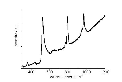
Figure 1. Average Raman spectrum obtained in the mapping of a surface on the SiSiC sheet (cf. Figures 2A and 2B).
The spectrum shown in Figure 1 shows a Raman spectrum of the SISIC sheet, obtained by averaging over all spectra recorded from the area shown in the video micrograph (Figure 2A). On a sloping background, signals are observed that can be assigned to silicon and silicon carbide. The bands assigned to silicon carbide are observed at Raman shifts of 770, 791 and 800 cm-1 (TO branch), and 970 cm-1 (LO branch). Band positions were obtained by curve fitting, with the use of Voigt profiles. The LO mode of SiC is superimposed on signals due to silicon that fall into the range of 940-1000 cm-1. Interestingly, at a band position of about 520 cm-1, where the TO mode of crystalline silicon is normally found, the line shape of the signal assigned to silicon is broadened and asymmetrically distorted. Such an effect has been reported in the literature for p-doped silicon [8].
It should be recalled that SISIC has a high electrical conductivity (typical volume resistivity: 102 – 103 Wcm). In addition, the silicon phase is heavily doped with impurities, due to the production method. Both these characteristics can explain the dispersive nature of the Raman band observed for the silicon subphase. The high electrical conductivity implies the existence of free carriers, which are excited by the laser. This excitation of the free carriers in semiconductors produces an electrical field, which under certain conditions couples with a phonon [6]. Now, two channels exist for a Raman process: The incoming photon may be scattered directly by the free carriers, which exist in a continuum of energy states; or it may be scattered by a phonon [9]. The first process results in the observation of a broad continuum in the Raman spectrum (note the sloping background recorded), whereas the latter process leads to the observation of a vibrational band. Due to the coupling between the free carriers and the phonon, the vibrational mode observed is shifted in its band position and changes its shape.
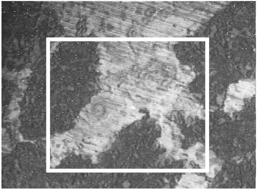
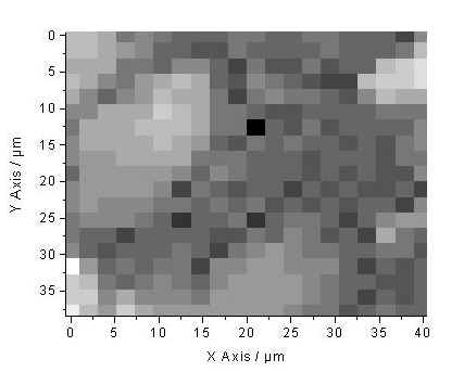
Figure 2. Video micrograph of the SISIC sheet. The area within the white rectangle was examined in the Raman mapping experiment. B: Raman map recorded on the SISIC sheet with a spatial resolution of 2 µm. The ratio ISiC/ISi, defined by intensity obtained in the wavenumber range 760 – 815 cm-1 (SiC specific) divided by intensity recorded in the wavenumber range 515 – 535 cm-1 (Si specific), is used to illustrate the distribution of Si-rich and SiC-rich regions. On a grey scale, light colours represent points with an high value of ISiC/ISi, whereas darker points mark the silicon-rich parts (low value of ISiC/ISi).
In Figure 2A, a video micrograph of the region investigated is shown. The results of the Raman mapping experiment performed at room temperature are displayed in Figure 2B. In the Raman map, the ratio ISiC/ISi, defined by intensity obtained in the wavenumber range 760 – 815 cm-1 (SiC specific) divided by intensity recorded in the wavenumber range 515 – 535 cm-1 (Si specific), is used to illustrate the distribution of Si-rich and SiC-rich regions. On a grey scale, light colours represent points with an high value of ISiC/ISi, whereas darker points mark the silicon-rich parts (low value of ISiC/ISi). With the results displayed in Figure 2B, it is demonstrated that Raman spectroscopy differentiates the two components of the SISIC material. Moreover, from a comparison of the video micrograph (Figure 2A) and the Raman map (Figure 2B), it may be inferred that the dark regions shown in the video micrograph contain mostly silicon carbide, whereas the light grey zones correspond to higher silicon content. For the example presented, a direct correlation between spectroscopical and morphological features can be established. But, in addition to optical microscopy, Raman microscopy offers detailed information on the constituents of this composite material.
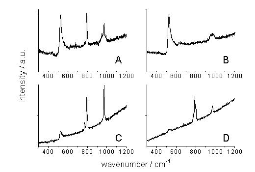
Figure 3. Raman spectra recorded at four different locations on the surface of the SiSiC sheet. Note the dispersion-type band profile recorded for the silicon component in traces A and B. Also, there are different fingerprints of the SiC subphase at different locations on the map, as exemplified by the spectra C and D.
In Figure 3, several example spectra taken from selected points of the SISIC sheet are shown. Differences between the spectra displayed in Figure 3 are clearly visible. In Figure 3A, the spectrum shown has features typical for silicon carbide. Band positions of the TO modes are found at 766, 790, 801. In addition, the LO mode is observed at 972 cm-1. These bands can be assigned to vibrational modes of the 6H-polytype of silicon carbide [2,3]. Additionally, a dispersive type signal is observed at a position of about 520 cm-1, where the first order Raman band of silicon would have been expected. A second feature, due to silicon, is observed as a broad feature in the range 935 – 1000 cm-1, with the aforementioned LO mode of silicon carbide at 972 cm-1 superimposed on this band. Interestingly, we note that this Raman band is not a dispersive type signal, but resembles the signal observed for polycristalline silicon. In Figure 3B, a spectrum of a point in the lower right corner of the area examined is shown where only features due to silicon are observed. Again, a dispersive type Raman band is observed. The spectrum given in Figure 3C indicates the presence of silicon carbide; in addition; an asymmetrically broadened profile around 520 cm-1 is observed with low intensity. The Raman band in Figure 3C is not so heavily distorted as the bands displayed in Figures 3A and 3B, respectively. The comparison of Figure 3C with Figure 3D shows that the band pattern recorded for the silicon carbide subphase differs between these two spectra, which were recorded at different locations on the SISIC sheet. The band profile recorded in the wavenumber region of the TO branch is slightly different, which can be explained by different linewidths observed. In addition, the intensity ratio of the TO and LO modes is different. This is attributed to differences in surface morphology at these sites.
The line shape observed for the silicon subphase may be described by the Breit-Wigner-Fano profile, which was derived to describe the effects of interaction of a discrete energy level with a continuum of states [10]. Dresselhaus and Dresselhaus [11] gave an especially convenient representation of the Breit-Wigner-Fano lineshape that will be used here for the description of the profiles shown in Figure 3. According to these authors, the lineshape, as a function of wavenumber,![]() , can be represented by the equation:
, can be represented by the equation:
(4) I(![]() ) = I0 [1+((
) = I0 [1+(( ![]() –
–![]() 0)/qG)]2 [1+(
0)/qG)]2 [1+(![]() –
–![]() 0)/G)2]-1
0)/G)2]-1
According to Ref. [8], I0 is a normalization factor (named intensity hereafter), ![]() 0 is the renormalized resonant wavenumber (band position), G is a measure of the linewidth, and q is the Breit-Wigner-Fano coupling coefficient. The magnitude of the coupling coefficient describes the extent of coupling to the continuum. If the value of q is a large number, the coupling to the continuum is weak, whereas a small value of q signifies strong coupling to the continuum. In the limit q -1 ® 0, equation (4) produces the Lorentzian lineshape. Equation (4) has been implemented into the Peak Fitting Module of the Origin 5.0 program package (Microcal Inc., Northampton MA, ). Results for the silicon band observed in spectra 3A – 3D are reproduced in Table 1. In case of the spectra analysed, the lineshape found for traces 3A, 3B, and 3C are typical for a strong coupling to the continuum, whereas the lineshape encountered for trace 3D is best described with a Lorentzian profile.
0 is the renormalized resonant wavenumber (band position), G is a measure of the linewidth, and q is the Breit-Wigner-Fano coupling coefficient. The magnitude of the coupling coefficient describes the extent of coupling to the continuum. If the value of q is a large number, the coupling to the continuum is weak, whereas a small value of q signifies strong coupling to the continuum. In the limit q -1 ® 0, equation (4) produces the Lorentzian lineshape. Equation (4) has been implemented into the Peak Fitting Module of the Origin 5.0 program package (Microcal Inc., Northampton MA, ). Results for the silicon band observed in spectra 3A – 3D are reproduced in Table 1. In case of the spectra analysed, the lineshape found for traces 3A, 3B, and 3C are typical for a strong coupling to the continuum, whereas the lineshape encountered for trace 3D is best described with a Lorentzian profile.
|
spectrum |
|
G [cm-1] |
q |
|
trace A |
517.4 ± 0.1 | 10.0 ± 0.2 | 3.0 ± 0.1 |
|
trace B |
518.0 ± 0.2 | 12.4 ± 0.2 | 2.7 ± 0.1 |
|
trace C |
518.1 ± 0.1 | 10.9 ± 0.8 | 3.0 ± 0.3 |
|
trace D |
526.3 ± 1.2 | 26.7 ± 3.7 |
Table 1. Raman band positions calculated for the silicon phase at the surface of the SISIC sheet. For the analysis of the silicon band observed in trace 3D, a lorentzian was used, whereas all other spectra were analyzed with the use of the Breit-Wigner-Fano lineshape.
A possible application of such a lineshape analysis is the estimation of the impurity concentration in the silicon phase. This has been already demonstrated for p- and n-doped silicon [8]. Alternatively, such an analysis may be used in the estimation of the electrical conductivity on a micrometer scale, which follows from the fact that signals with dispersion-type contribution are recorded only for the silicon phase, and we might infer that the silicon phase is responsible for the high electrical conductivity of the SISIC ceramic, which exceeds the value found for silicon carbide roughly by two orders of magnitude. But the lineshapes observed in heavily doped semiconductors are sensitive to the type of doping present. Only with p-doped silicon, the lineshape distortions described here are observed, whereas a different behaviour would have been observed with heavily n-doped silicon [8]. On the other hand, it is known from a characterization of n-doped SiC single crystals that the lineshape of the LO mode can also be described with the use of equation (1) [12]. From the results of this study, we conclude that p-doped SiC shows no features typically observed for p-doped silicon, but we have to be aware of the fact that SiC is spectroscopically “silent” does not necessarily prove that only silicon is responsible for the electrical conductivity.
Raman mapping at elevated temperatures
Raman spectroscopy performed at different temperatures will provide interesting information concerning the mechanism of electrical conduction in the SISIC material. Because SISIC is a metallic conductor in the temperature range investigated, it is expected that the coupling parameter q increases, and a near lorentzian lineshape should be observed at high temperatures for the TO mode of silicon. On the other hand, examination of technical ceramics under in-situ conditions at elevated temperatures may yield information upon phase transformations and structural changes taking place. SISIC serves here as an ideal sample to test the method proposed, since it should be stable at temperatures up to 1500 K, even under oxidative conditions.
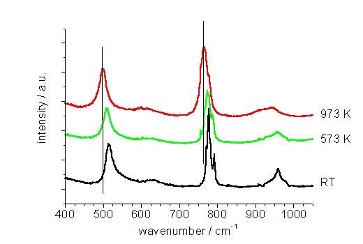
Figure 4. Averaged Raman spectra recorded at different temperatures in the in-situ cell. With increasing temperature, the band profiles broaden and shift to smaller wavenumber.
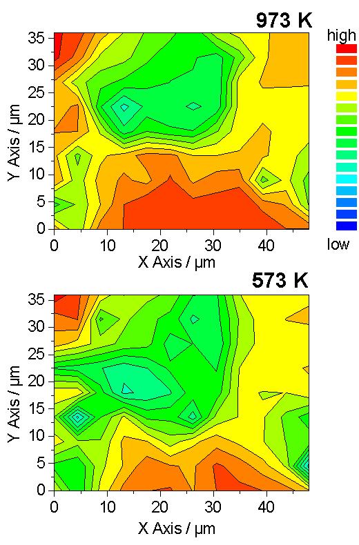
Figure 5. Raman map obtained at a temperature of 573 K (lower graph), compared with the map sampled at a temperature of 973 K (upper graph).
The results of a first experiment are shown in Figures. 4 and 5. In Figure. 4, Raman spectra of the SISIC material recorded at room temperature, 573 K and 973 K are shown. The spectra presented are averaged spectra constructed from all spectra recorded on a defined area. The Raman maps of this area, recorded at 573 K (lower graph) and 973 K (upper graph), are compared in Figure 5. The inspection of Figure 4 reveals that the band positions of both silicon and silicon carbide vibrational modes decrease with increasing temperature. The band position of the silicon TO mode and associated parameters obtained from curve fitting are listed in Table 2. The band position decreases by 12 cm-1, whereas the linewidth obtained is nearly constant, with a value of about 12 cm-1. The coupling coefficient q changes in the expected way. With an increase of the temperature of about 300 K, the coupling coefficient doubles, whereas a further increase of 400 K in temperature results in a coupling coefficient of about 2E19, which means that at this temperature, the lineshape is essentially a lorentzian. In this way, it has been confirmed with Raman spectroscopy that SISIC shows metallic conductivity in the temperature range investigated.
|
T / K |
|
G [cm-1] |
q |
|
294 |
512.4 ± 0.2 | 11.9 ± 0.2 | 4.7 ± 0.2 |
|
573 |
508.1 ± 0.2 | 12.6 ± 0.2 | 10.0 ± 0.7 |
|
973 |
499.1 ± 0.1 | 11.5 ± 0.2 | 2E19 |
Table 2. Raman band parameters calculated for the signals due to the silicon phase at the surface of the SISIC sheet, recorded at temperatures indicated. All spectra were analyzed with the use of the Breit-Wigner-Fano lineshape.
The Raman maps displayed in Figure 5 demonstrate that it is possible to use Raman microscopy for the characterization of the SISIC sheet under controlled conditions. The lower map (Figure 5A) was recorded at a temperature of 573 K, whereas the upper map (Figure 5B) has been obtained at a temperature of 973 K. Again, the intensity ratio ISiC/ISi is used to illustrate the distribution of the components. For each map, the bandpass employed in the calculation of the intensity ratio was adjusted to compensate for the shift of band position discussed above. On the colour scale employed, the silicon-rich parts (low value of ISiC/ISi) are drawn in blue and green colours, whereas areas rich in SiC are drawn in orange and red colours. For both maps, an area rich in silicon is located in the upper part of the map, bordered by a upper left corner rich in SiC, which prevails also in the lower middle of the map. In the lower right corner, an area rich in silicon is found. This distribution is observed for both maps, though there exist some minor differences. At present, it is not known if these differences are significant, since the data set recorded is not very extensive.
Conclusions
It has been shown that Raman microprobe techniques have a potential as a characterization method for composite ceramic materials. The method used here is capable to differentiate the components of the ceramic composite material, silicon infiltrated silicon carbide. Further information on the nature of the silicon phase, which is heavily p-doped, has been obtained as well. A qualitative explanation for the line shape observed has been given, and results of a lineshape analysis using Breit-Wigner-Fano profiles illustrated the change in the coupling of the 520 cm-1 Raman mode of silicon to the continuum of free carriers in the SISIC ceramic. In addition, it has been demonstrated that in case of the SISIC material, it is possible to use Raman microscopy for the characterization of technical ceramics at elevated temperatures under controlled atmosphere. This is regarded as one of the principal advantages that Raman microscopy offers in the characterization of such materials.
Acknowledgements
Thanks are due to Friederike Geiger and Eugen Groth for cutting the ceramic material. I also acknowledge a helpful discussion on the subject with Otto Haas.
References
-
A. Sonntag, Am. Ceram. Soc. Bull. 76, No. 11, 51, (1997).
-
J. A. Freitas Jr., “Phonons in SiC polytypes”, in: Properties of silicon carbide, G. L. Harris, Ed., (INSPEC, London, 1995), Chap. 2.2, pp. 21-28.
-
S. Nakashima, H. Harima, Phys. Stat. Sol.(a), 162, 39, (1997).
-
A. Lynen, R. W. Steinbrech, H. Nickel, Grundlagen zur Infiltration von SiC-C- Verbundkörpern mit Silicium, (Ber. Forschungszentrum Jülich, Vol. 3227, 1996).
-
J.-C. Panitz, A. Wokaun, Appl. Spectrosc., 1997, 52, 1252, (1998).
-
G. Abstreiter, M. Cardona, A. Pinczuk, “Light scattering by Free Carrier Excitations in Semiconductors “, in: Light Scattering in Solids IV, M. Cardona and G. Güntherodt, Eds. (Springer Verlag, Berlin, 1982), Chap. 2.
-
J.-C. Panitz, Appl. Spectrosc., 1997, 51, 1073, (1997).
-
R. Beserman, M. Jouanne, M. Balkanski, in: 11th International Conference on the Physics of Semiconductors Proceedings, (Elsevier, Amsterdam, 1972), Vol.2, p. 1181.
-
M.V. Klein, in: Laser Optics of Condensed Matter, eds.: Elsa Garmire, Alexei A. Maradudin, Karl K. Rebane, Vol. 2, pp. 137-144 (140), Plenum Press, NY 1991.
-
J. F. Scott, Rev. Mod. Phys., 46, 83, (1974).
-
M. S. Dresselhaus, G. Dresselhaus, “Light scattering in Graphite Intercalation Compounds”, in: Light Scattering in Solids III, M. Cardona and G. Güntherodt, Eds. (Springer Verlag, Berlin, 1982), Chap. 2, pp. 32-33.
-
H. Harima, T. Hosoda, S. Nakashima, in: Proceedings of the 7th International Conference on Silicon Carbide, III-Nitrides and Related Materials, eds.: G. Pensl, H. Morkoç, B. Monemar and E. Janzén, p. 449, TransTech Publications, 1998.
Received 6th August 1999, received in revised format 14th August,
accepted 14th August 1999
REF: Panitz J-C. Int. J. Vib. Spect., [www.irdg.org/ijvs] 3, 4, 5 (1999)